The following integrated circuits are used. Datasheets are available for all parts, except for the CDP1861. The link there takes you to a descriptive article.. :-
The connector is a single sided 22 way 0.156" pitch type. The bottom connectors (those nearest the edge of the machine) are the only ones used. The enumeration is from the left side of the board - the side where the tuner, switches and RF lead are.
However, plugging Cartridges in isn't that simple. A Studio II Cartridge
has a metal comb that shorts out all the cartridge pins normally. This
is pushed up and out of the way when the cartridge is inserted into the
Studio 2 (by the two poles the cart fits onto). If you look up the hole
you can see the edge of the lifting bar. [The best way to bodge this is
to stick a couple of pieces of dowel in there].
|
|
|
Description |
|
|
|
|
|
|
|
|
|
|
|
|
|
|
|
|
|
|
|
|
|
|
|
This pin is connected to the chip select (high) pins on the two right most CDP1831 ROM Chips which hold the "game" code, the ROM data between $400 and $7FF. This line is normally pulled to logic '1' via a resistor. In cartridges, this pin is normally connected to the adjacent pin, pin 7, ground, disabling those two ROM chips. |
|
|
|
|
|
|
|
|
|
|
|
|
|
|
|
|
|
|
|
|
|
|
|
|
|
|
|
|
|
|
|
|
|
|
|
|
|
|
|
|
|
|
|
|
|
|
|
|
|
|
|
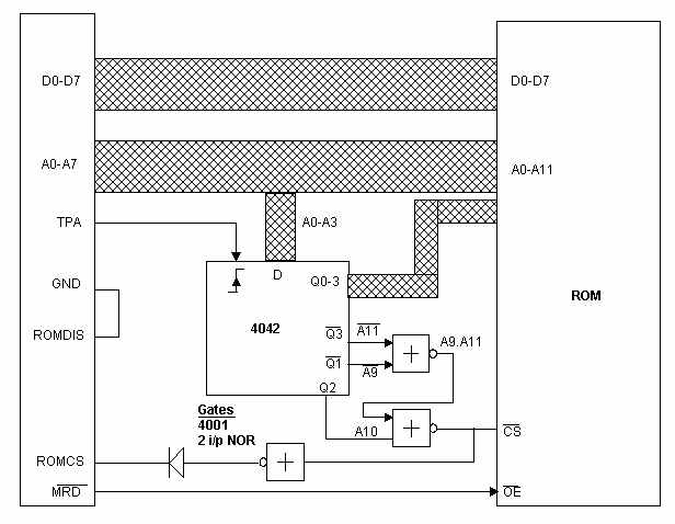
This signal is a positive going High address latch , it is connected to pin 23 of the CDP1831 ROMs. It is a simple logic circuit. First TPA is inverted (4001 pins 8,9,10), then it is exclusive NORed with MRD (4001 pins 1,2,3). This gate only produces a logic '1' when MRD is logic 0, and TPA is logic 1, i.e. it goes from 0->1 when the high address byte is on address lines 0-7. |
|
|
|
|
|
|
|
The active low memory read line direct from the 1802 CPU. |
|
|
|
This is a logic '1' going Chip select line from the ROMs inside the cartridge. This line should go to logic '1' when the ROM is selected and enabled. See the section on "RAM Decoding". |
Then by following the sequence listed below one can read the contents of the ROM. An important catch to watch for is that the ROMs are self-decoding. This means that they recognise their own addresses, so if you do it this way it is likely nothing will be read outside the range $0400-$07FF (and the MSBs of the address will probably be significant too).
It is theoretically possible for ROM to be stored between A00-BFF and E00-FFF, but to my knowledge no cartridge has done this ... yet. There is a standard cartridge PCB which has spaces for 2 CDP1831 Integrated Circuits (and the 2 Diodes that wire into the big OR gate to disable RAM). I would bet that all of these are mapped onto 400-7FF ; but it isn't mandatory for them to do so. One thing I have learnt from emulator development is never to assume any design or program will be sane.
The design for the cartridge dumper is here. This has now been built and tested by me.
Note: this worked perfectly on my (well John's) RCA Studio 2. It might not work on others, but I don't see why it shouldn't. Any damage done to your RCA Studio 2 as a result of doing this is just .... bad luck, sorry. As far as I can tell John's still works , it powers up, beeps, and seems to be generating the correct signals. I can't absolutely check it as I'm in PAL land and the S2 is an NTSC one. But it is producing the right signals and the right sounds, so it is almost certainly working as far as the video circuitry.
Definitely don't try this if you aren't reasonably handy with a soldering iron.
Cut the power to the 1802. This involves cutting three tracks. Top and Bottom of pin 40 on the 1802 (Vdd) and the top track of pin 12 (Vcc). Connect them together and connect them through a switch to a power source ; the resistor above the 1802 (right side) is suitable as it is the pull up resistor for WAIT (pin 2).
Connect flying leads to A0-A7,DB0-DB7, 5V and 0V (don't use the RCA Power) and MRD. By far the safest places to connect these is on the cartridge connector (see above)
Connect flying leads to TPA and TPB. You will have to connect these directly on the board.
When the power is cut to the 1802 and the rest of the board powered up the buses become open collector (I *think* this is what happens) and effectively "float". When this happens the A0-A7,MRD,TPA and TPB lines can be controlled via an I/O device, [I used an Atmel AVR Microcontroller on the STK200 Prototyping Board, ask if you want the software] and the DB0-DB7 lines read to retrieve data. For precise details of the protocols, read the Harris/Intersil Datasheet but in brief summary :-.
Initially, TPA = 0 and MRD = 1.
When you've finished, just remove the I/O connector plug, and switch power back to the 1802, and it should work as well as it ever did.
Firstly, the ROMs are CDP1833CE types. These are newer, 1k x 8 ROMs. This suggests his machine has an extra 1k of ROM, and also that the decoding is different ; probably the extra system ROM will go in the space from A00-FFF which is not used at present (except for the RAM Mirror).
Secondly, there is an extra CDP1822NCE (256 byte x 4 RAM chip). Logic would suggest that this colour data is piggybacked on to the 256 byte of video data, thus this machine has effectively an 8 pixel x 32 line colour resolution. This is totally feasible - the chip could be read using the same read pulse as the main RAM and then it could be read and fed into the video circuitry.
Three of the bits would be Red,Green and Blue colours. The other could be unused, intensity or flashing, I don't know.
Thanks to Oliver Boisseau, I have discovered that the Hanimex MPT02 is a colour machine as well. It will run S2 ROMs (Tennis, anyway) but does so in two colour, but not black and white.
Actually, this is wrong, but right in practice.. What really is the
case is that the ROM is where I say here, in page 0 (e.g. 0000-07FF) and
not anywhere else. The RAM is all over the place. See section 17 on the
decoding circuitry. Bizarrely you *could* have a game which was 63.5k in
length if you really wanted to !
| Address Range | Contents | Notes |
| 000-2FF | ROM | RCA System ROM : Interpreter |
| 300-3FF | ROM | RCA System ROM : Always present |
| 400-7FF | ROM | Games Programs, built in (no cartridge) |
| 400-7FF | Cartridge | Cartridge Games (when cartridge plugged in) |
| 800-8FF | RAM | System Memory, Program Memory etc. |
| 900-9FF | RAM | Display Memory |
| A00-BFF | Cartridge | Available for Cartridge games if required, probably isn't. |
| C00-DFF | RAM/ROM | Duplicate of 800-9FF - the RAM is double mapped in the default set up. This RAM can be disabled and ROM can be put here instead, so assume this is ROM for emulation purposes. |
| E00-FFF | Cartridge | Available for Cartridge games if required, probably isn't. |
The hardware is described in greater detail here.
In theory, the RCA can support a resolution of 64 horizontal and up to 128 lines vertically. In reality, however, the display is a memory mapped type between 900 and 9FF, 64 pixels by 32, 8 bytes per line. This is what the code in the ROM supports. Theoretically, you could replace the Interrupt driver with a different one, but I doubt any cartridge did this.
The sound circuit is based around an NE555, driven in Astable mode, with Ra = 400k, Rb = 480k and C = 1.8pf. This gives a working frequency of 625 Khz. To complicate things, the control line (pin 5) of the 555 is connected to 0v via a 10uf Electrolytic capacitor. The effect of this is to decay the frequency to about half its standard value in about 0.4 seconds. This gives the peculiar "warpy" effect you hear on power up.
Also, I believe there is a capacitor charging circuit to extend the length of the first "beep" on power up. This is programmed for only 0.08s, but is clearly longer than that.
The strobing singla is obtained by inverting TPB (4001 gates 4,5,6) and exclusive Noring it with the output of Q1 (see "Decoding"). The net effect of this is that it it strobes when TPB = 1, and the "stored" value of N1 is 0.
| 4042 "D" Pin | 1802 Signal | Description |
| 4 | N1 | Latches the value of N1, used for strobing the keyboard hardware |
| 7 | 0v | Not used |
| 13 | MA0 | Address bit 8 |
| 14 | MA1 | Address bit 9 |
For full connections refer to any standard CMOS Datasheet.
Games are kept between 400 and 7FF. When a cartridge is plugged in, it replaces this part of the memory map. The "Pseudo Machine Language" from 300-3FF are always available. Most of it is not of any great use.
| A7 | 1 | --------\_____/--------- | 24 | 5v |
| A6 | 2 | 23 | Clock | |
| A5 | 3 | 22 | NC | |
| A4 | 4 | 21 | CS1 | |
| A3 | 5 | 20 | CS2 | |
| A2 | 6 | 19 | !MRD | |
| A1 | 7 | 18 | CEO | |
| A0 | 8 | 17 | D7 | |
| D0 | 9 | 16 | D6 | |
| D1 | 10 | 15 | D5 | |
| D2 | 11 | 14 | D4 | |
| 0v | 12 | -------------------------- | 13 | D3 |
| A3 | 1 | --------\_____/--------- | 22 | 5v |
| A2 | 2 | 21 | A4 | |
| A1 | 3 | 20 | R/W | |
| A0 | 4 | 19 | !CS1 | |
| A5 | 5 | 18 | OD | |
| A6 | 6 | 17 | CS2 | |
| A7 | 7 | 16 | DO4 | |
| 0V | 8 | 15 | DI4 | |
| DI1 | 9 | 14 | DO3 | |
| DO1 | 10 | 13 | DI3 | |
| DI2 | 11 | -------------------------- | 12 | DO2 |
The majority of the functions and connections are obvious. Those which
are not are as follows :-
| Pin | Function | Connection |
| 17 | CS2 | Enables RAM chip when logic '1'. This is connected to the !Q3 line (left 2 RAM chips) or the Q3 line (right two RAM chips) from the 4042 : the latched value of A8. This selects the upper or lower 256 bytes of RAM. |
| 18 | OD | Output is disabled when logic '1'. This is connected to !MRD from the 1802, so the output is enabled when !MRD is logic '0', i.e. a read is taking place. |
| 19 | !CS1 | Enables RAM chip when logic '0'. See decoding part later |
| 20 | R/!W | Controls read or write action. Connected to !MWR on the 1802. |
The function of this circuitry is to put a logic '0' on the RAM Chip invert select line (thus enabling it) provided all the following are true :-
Of course, if you link pins 6 and 7 on the cartridge connector this disables the 2 right hand ROMs, thus allowing another ROM to appear between 0400 and 07FF.
This could cause chaos. Technically, I believe, ROM can be placed anywhere between 0400 and FFFF. The CDP1831 ROM chips can be programmed to fit anywhere in this map, and because of the ROMs being able to physically disable the RAM by driving Pin 22 to logic '1' they can also do things like map out the RAM.
I know that a ROM image always begins at $0400 and it would be common sense to use the 1k of ROM between 0400 and 07FF for 1k programs. However, any additional ROM (are there any >1k cartridges ?) can go at any address (except 0800-09FF as this would stuff the video interrupt routine).
This is the reason for the rather peculiar cartridge format. It is designed to put ROM anywhere.
Building a replacement cartridge of up to 2.5k in size should be relatively
simple. Firstly, latch the lines A0-A3 on the 0-1 transition of TPA using
a 4042 latch. This provides the bits A8-A11 of the address. A 4001 gate
decodes the relevant addresses (400-7FF,A00-FFF). A line returns via a
signal diode to the "Disable RAM" diode OR gate.
An important note for assembly language programmers is that the interrupt routine will modify certain registers and memory locations. See the BIOS disasssembly for more details.
The carts binaries are in a special format ; this is documented at the main site and a program called mcart.zip will produce files in this format.
Be careful when powering up the S2 from a seperate source. Do not rely on the 7805 regulator on the circuit board to limit the board voltage to 5V ; it doesn't seem to work that way. Power up by connecting 5v to the cartridge plug solder points.
And that's it !