The photo at the top of this page illustrates what can be done with
the original 256 bytes of memory in the Elf when the Pixie graphics system
is added. In this article, we will show you how to install and program
the Pixie system to produce this type of graphics.
|
The selected segment of memory appears on-screen as an array of small squares that represent individual memory bits. If a memory bit is a 1, the appropriate square will be white, while if a bit is a 0, the square will be dark. Changing the bit pattern within the memory will change the pattern that appears on-screen. You can store several different bit patterns (pictures) in memory and, using software, display them successively onscreen to produce animation effects. Low-resolution alphanumerics can also be created.
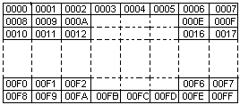
Since the basic Elf has only 256 bytes of memory, we will show how to display the entire memory on the screen. The memory is mapped as shown in Fig. 1, in an array of 64 spots wide (eight bytes with eight bits/byte) by 32 spots high to make a total of 256 bytes.
The byte at M(0000) is displayed at tthe upper-left of the screen; each
row on the screen is equivalent to eight memory bytes. Byte M(00FF) appears
at the bottom-right of the screen.
The 1861 chip uses the same clock as the 1802 µP chip to trigger internal counters to provide the TV-like composite sync at pin 6. The graphics display is directly refreshed from the memory 60 times each second, accomplished by an interrupt request sent to the 1802 at the same rate.
When the 1802 receives the interrupt request, it temporarily stops the program it is executing and immediately branches to the interrupt routine previously stored in memory. This branch occurs when P is automatically set to 1 and X is set to 2. The interrupt routine program counter is always R1, which must be set to the address of the interrupt routine before the 1861 is activated and starts sending interrupts to the 1802. A pulse from NO is sent to pin 10 of the 1861, permitting this chip to start sending interrupts. A 69 instruction can be used to generate the 1861 activation pulse. The 1861 is always turned off when the Elf is stopped with the RUN switch down.
In the program shown in Table I, R1 is set to the address of the interrupt routine at M(0011), R2 is set to the address of the work area (or stack) used subsequently for byte storage, R3 is set to the main program starting at M(002D), and setting P=3 causes a branch to M(002D) with R3 as the program counter. The main program permits entry of the bytes at any time via the Elf's toggle switches. This permits you to see what is happening to the CRT screen as memory bytes are changed. The program loops on itself until an interrupt signal is generated by the 1861, activated by the 69 instruction at M(002E).
Exactly 29 machine cycles after the initiation of the interrupt routine,
the 1861 requests eight sequential memory bytes by putting down the DMA-OUT
(pin-2) request line for eight bytes (eight machine cycles). This automatically
causes eight memory bytes, addressed by R0, to be sequentially fetched
and transferred to the 1861 via the data bus. Note that the C4 instructions
at M(0015) are special no-op instructions that re-quire three cycles for
each execution. These are used only to provide the delay required to between
the beginning of the interrupt routine and the first eight-byte
DMA request generated by the 1861 display circuits.
Each of the eight display refresh bytes requested by the 1861 is internally converted to a bit serial form and used to provide the luminance (brightness) pulses that come out of the 1861 at pin 7. The actual raster display consists of 262 horizontal lines for each frame, and there are 60 frames per second. Each display spot is four raster lines high, which means that each eight-byte display row must be repeated four times. With the interrupt routine, R0 is initially set to M(0000) to M(0007) to be fetched and displayed. The time of each raster line is exactly 14 machine cycles to permit the transfer of eight bytes (eight cycles) plus the execution of three two-cycle instructions during each raster line time. Following the eight DMA cycles required to refresh the first eight bytes, R0 is restored to its original value so that it remains pointing at the same eight bytes.
The E2 20 A0 instructions at M(0020), M(0023), and M(0026) are used to occupy six machine cycles between the DMA requests and to restore R0 to its initial value before incrementing it by eight during the eight-byte DMA request. The 20 instruction decrements R0.1 back to its initial value if a 256-byte page boundary was crossed during the preceding eight DMA cycles.
After the first group of eight bytes has been displayed for four raster line times, R0 is permitted to advance to the next group of eight bytes to be displayed. This process is continued until 32 groups of eight bytes each (256 total) have been displayed. At this time, the circuits in the 1861 chip cause line EF1=1 (at pin 9) and the interrupt routine terminates.
Since the 1802 and the 1861 clocks must remain synchronized, none of the three-cycle instructions described in the 1802's user's manual should be used in programs that run concurrently with this display. The only exception is the use of the C4 instruction in the interrupt routine.
The sample program given in Table I was designed to run in expanded-memory systems as well as in the basic 256-byte Elf. In the expanded system, just change the bytes at M(0019) and M(001C) so that R0 initially points to any 256-byte segment of the memory you wish to display on the raster. You can write any other main program to run concurrently with this interrupt routine.
The 1861 chip can also be used to display any number of memory bytes from eight to 1024 by rewriting the interrupt routine. For example, change the byte at M(0024) from 20 to 80, and you will see 512 bytes displayed on the CRT screen as 64 spots horizontally by 64 spots vertically. If you have only 256 bytes of memory in your system, you will ass the same 256 bytes repeated twice on the screen. When displaying 512 bytes, each spot represents half the height of those displayed when 256 bytes are displayed.
One of the main advantages of mapping main memory directly into the
monitor or TV raster is the ability to manipulate the display using the
normal instruction set. In systems that employ an external frame buffer
for refresh, specialized instructions are required to change the buffer
contents. The buffer memory also costs more money. With the refresh buffer
approach toward animation, you must store two picture patterns in memory
and alternately transfer them to the buffer memory. Using the Pixie graphics
display described here, you store the same two-picture patterns in memory
but you need only change the initial value of R0 to alternately display
them. Not only do you save the cost of a refresh buffer, you can greatly
simplify the programming.
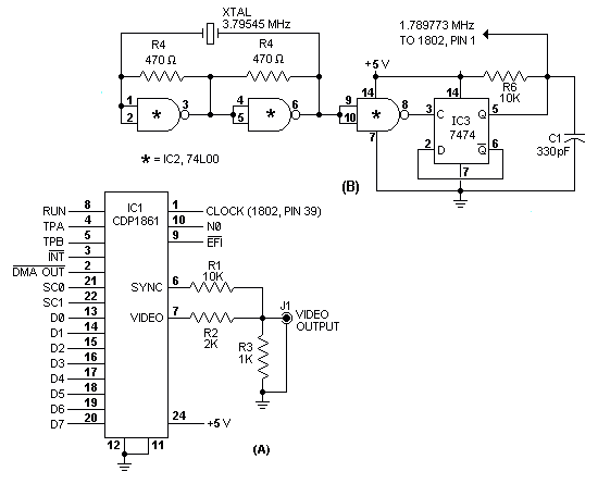 |
Fig 2. Video display chip connections are shown at (A), Optional circuit
to replace original Elf crystal is at (B).
 |
Listing : the driver program for the Pixie display. Note : this does
NOT
preserve DF !
| 0000 | 90 | GHI R0 | P = R0 = 0, so sets D = 0 |
| 0001 | B1 | PHI R1 | R1.H = 0 |
| 0002 | B2 | PHI R2 | R2.H = 0 |
| 0003 | B3 | PHI R3 | R3.H = 0 |
| 0004 | B4 | PHI R4 | R4.H = 0 |
| 0005 | F8 2D | LDI 2D | R3.0 = Main |
| 0007 | A3 | PLO R3 | |
| 0008 | F8 3F | LDI 3F | R2.0 = Stack |
| 000A | A2 | PLO R2 | |
| 000B | F8 11 | LDI 11 | R1.0 = Interrupt routine |
| 000D | A1 | PLO R1 | |
| 000E | D3 | SEP R3 | Go to main loop |
| 000F | 72 | LDXA | Restore 'D' register |
| 0010 | 70 | RET | Return from interrupts and re-enable. |
| 0011 | 22 | DEC R2 | Interrupt routine begins here. Save (X,P) on stack |
| 0012 | 78 | SAV | |
| 0013 | 22 | DEC R2 | Save D on stack |
| 0014 | 52 | STR R2 | |
| 0015 | C4 | NOP | 9 Cycles. Display starts 29 cycles after interrupt |
| 0016 | C4 | NOP | |
| 0017 | C4 | NOP | |
| 0018 | F8 00 | LDI 00 | R0 = 0000 (video from here) |
| 001A | B0 | PHI R0 | |
| 001B | F8 00 | LDI 00 | |
| 001D | A0 | PLO R0 | |
| 001E | 80 | GLO R0 | Refresh loop ; preserve line start address |
| 001F | E2 | SEX R2 | |
| 8 DMA Cycles | |||
| 0020 | E2 | SEX R2 | |
| 0021 | 20 | DEC R0 | |
| 0022 | A0 | PLO R0 | Re-fixes the correct display position |
| 8 DMA Cycles | |||
| 0023 | E2 | SEX R2 | |
| 0024 | 20 | DEC R0 | |
| 0025 | A0 | PLO R0 | Re-fixes the correct display position |
| 8 DMA Cycles | |||
| 0026 | E2 | SEX R2 | |
| 0027 | 20 | DEC R0 | |
| 0028 | A0 | PLO R0 | Re-fixes the correct display position |
| 8 DMA Cycles | |||
| 0029 | 3C 1E | BN1 1E | Go back and do another 4 scan lines if display not finished |
| 002B | 30 0F | BR 0F | Return from interrupt if no more video |
| 002D | Main program here. |